
My Favorite Class Last Term
Wouldn’t it be neat to look at something magnified to tens of thousands its normal size—so much that you can see the individual hair follicles on an ant (and realize it’s just as furry as a dog)? Or to fabricate an LED from scratch, doping the semiconductor and etching out the contacts, all to be rewarded by a tiny yet brilliant red light? Or to design a microfluidic device, drawing it in AutoCAD, making the mold out of a silicon wafer, and after producing each polymer layer, watching blue ink flow through the tiny channels?
Yes, yes, and yes, as I learned last term in APh 109, Introduction the Micro/Nanofabrication Laboratory. I took the class to fulfill one of therequirements for the electrical engineering major. There were no lectures; instead, groups of three or four of us met two evenings each week with a TA to do the labs. My group actually included my chemistry TA from last year, since graduate students also take the class to learn fabrication methods. Homework consisted of background reading and lab reports.
Our first project was to fabricate LEDs, or light emitting diodes, which are used in light bulbs, Christmas lights, and many other. If you’ve taken physics, you may have heard of doping, a practice used to make LEDs, among many other semiconductor-based electronic devices. Doping makes a semiconductor into more-or-less a conductor by adding extra free charges which can move around, i.e. carry current. When I briefly learned about doping in high school, I imagined the process to be unimaginably complex and precise. However, the technique we used, thermal diffusion, was surprisingly simple. We just put the semiconductor chip into a container with a piece of material containing the element we wanted to dope with, heated them up really hot, waited a while, and that was that. We now had a p-type semiconductor.
One of the LEDs we fabricated on the chip. The shiny circle on top is a thin layer of gold which served as an electrical contact for powering the LED.
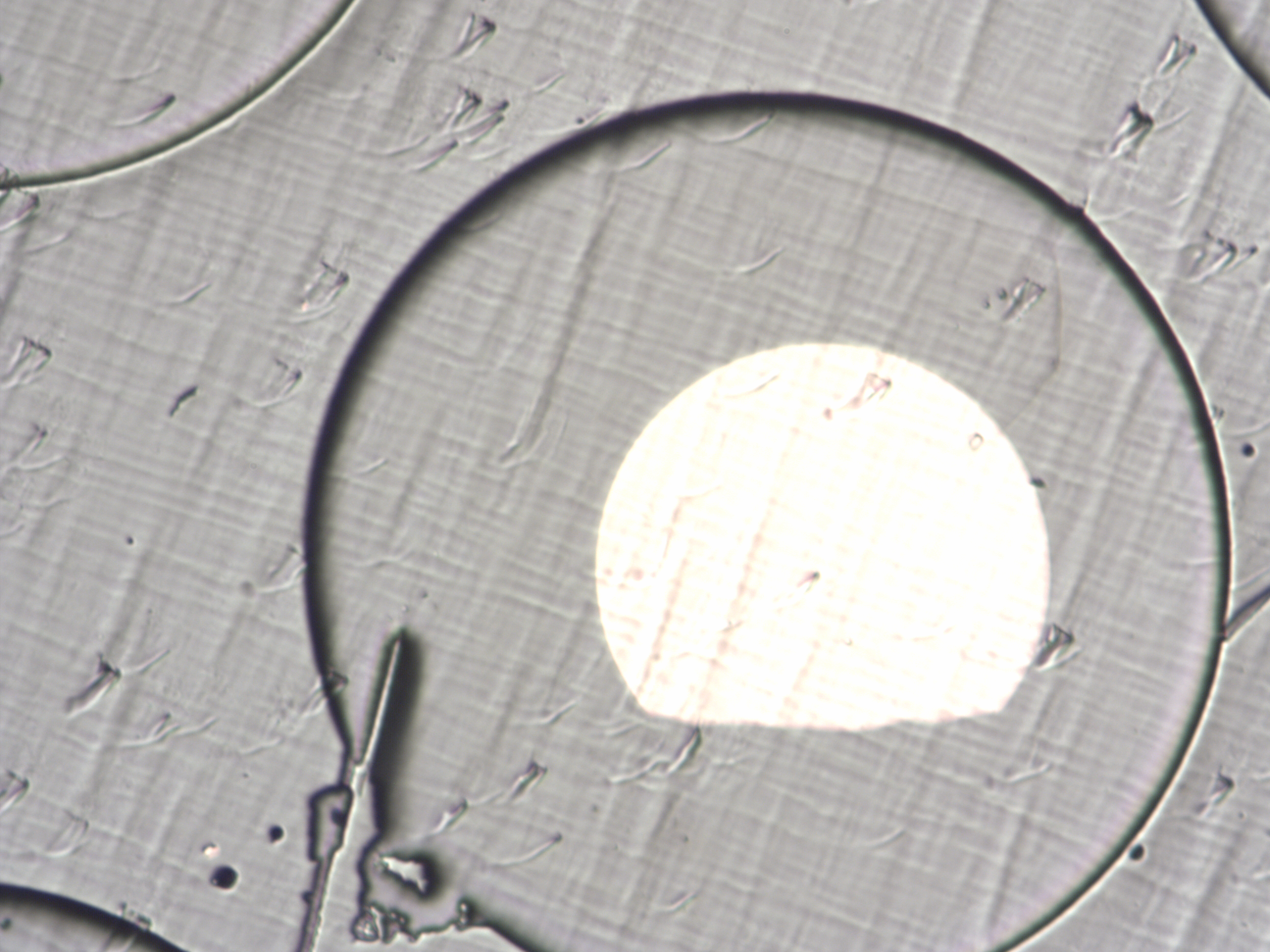
Our next project was electron-beam lithography. Electron beam lithography, or EBL, is a method for drawing tiny shapes on a silicon chip. To do EBL, you coat a chip with drops of a particular liquid called photoresist, heat it up until the liquid gels, and then use a machine to shoot electrons at the surface, as if coloring in the region you want to erase the photoresist from. Being bombarded by electrons changes the solubility of the photoresist, and so afterward, when you wash the chip with a particular chemical, you’re left with the desired pattern.
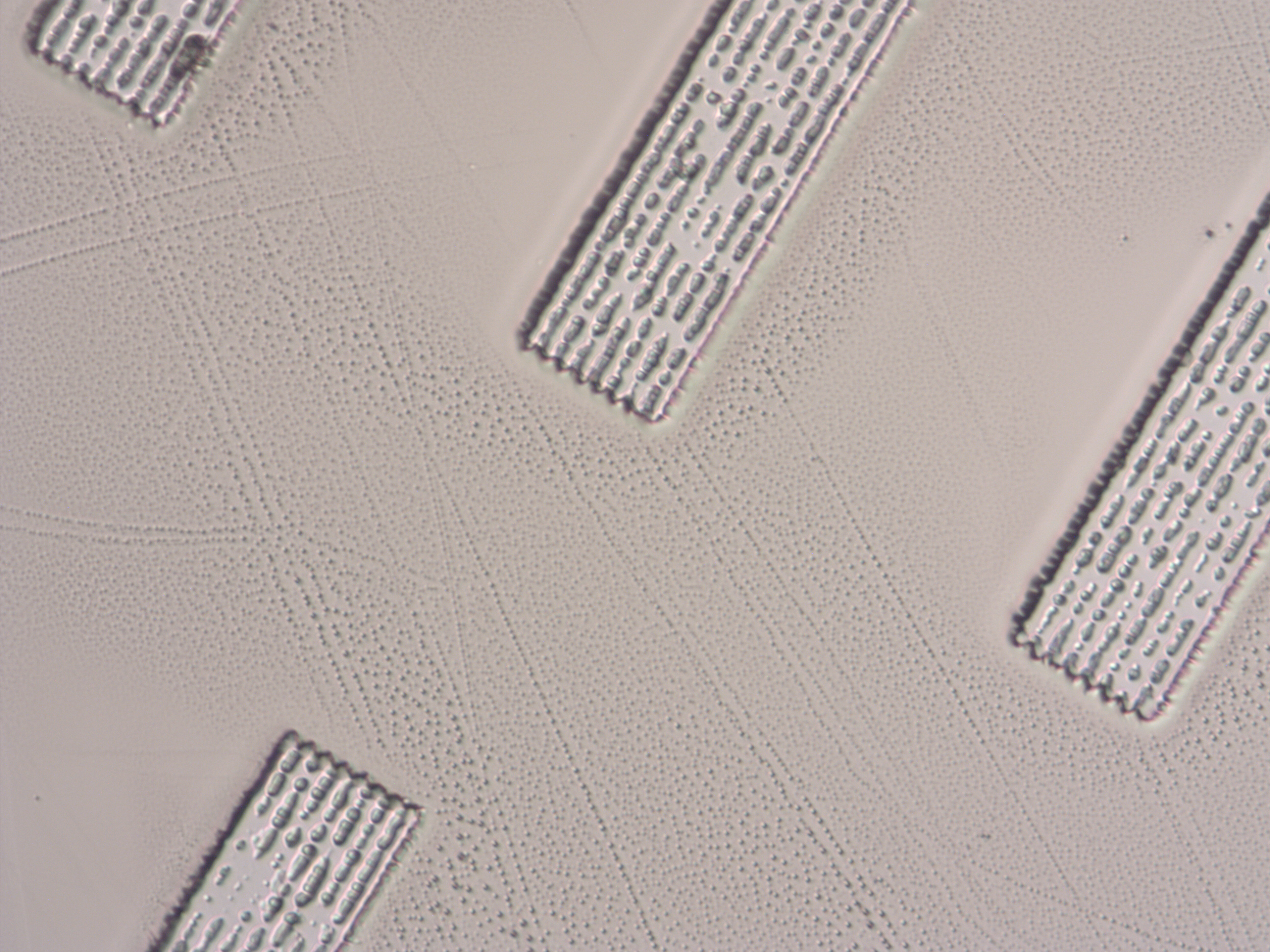
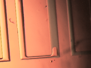
In another project, we took this a step further, and instead of stopping with the design in photoresist, we actually etched it into the silicon chip. To do this, we let the chip sit in a really nasty chemical which eats into silicon but can’t get through the photoresist. After washing everything off, the pattern was etched into the chip itelf. For this project, we used a template pattern—some boring rectangles.
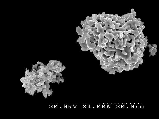
The next project, using a scanning electron microscope, didn’t involve designing or building anything, but was my absolute favorite. Here’s why:
The last project I’m going to describe is microfluidics. Microfluidic devices are, simply, devices that handle microliters (cubic millimeters) of liquid. They’re used for a variety of purposes, such as sorting cells for molecular screening or drug discovery. Our device was made from a clear, firm but squishy polymer. It had channels cut out inside it and inlet holes for injecting liquid with tiny syringes. We made the molds for the polymer layers out of silicon chips, etching out our designs using the same techniques as in past projects.
I generally enjoy lab classes, but this one was particularly fun because the projects involved buzzwords like “microfluidics,” “etching,” and “scanning electron microscope,” which I’d heard before in research seminars and held in a kind of distant awe. It was exciting to get to actually use these techniques that are involved in the cutting edge of research.


